The pre-Christmas period seems to be infamous for graphics technology launches, and no Christmas in recent memory will be quite so frenetic as this - last month saw the announcement of the new AMD cards, and this month brings not only the announcement, but the actual launch of a new NVIDIA card: the GTX580.
Though we speculated that this is a knee-jerk reaction to the AMD cards, rumoured to launch on the 22nd of November in less than two weeks, NVIDIA insist otherwise. We spoke with Jason Paul, Product Manager for the GTX580 for the APAC region, who explained that “[NVIDIA] felt with GTX480 we could’ve done better with power and acoustics. Those were two areas we were looking at in our next generation of products”.

Jason continued,“GTX580 is continuing to enhance and build upon [the GTX480] with more geometry horsepower, and allows developers to create incredible terrain and characters”, and it certainly seems like they've put some hard work into the Fermi core. Official specifications have been confirmed as leaked by an overwhelming number of sites, and appear in full below:
The GTX580: back to the drawing board
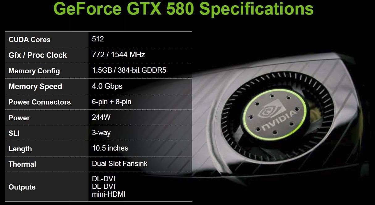
As can be seen above, the GTX580 boasts the full amount of CUDA Cores possible within the Fermi architecture, suggesting that the core now sports a total of 16 functional Streaming Multiprocessors which, as we explained in our initial GTX480 review, give it a total of 512 processing cores:
Inside each GPC resides a total of four large blocks called Streaming Multiprocessors, or SMs. These SMs each contain 32 CUDA Cores, the processors that do the actual calculation work, though it appears that a single SM in the GF100 is deactivated. The fifteen functional SMs add up to a total of 480 CUDA Cores.

Though the architecture itself remains largely unchanged, the code-name is GF110; ten higher than the initial release. Its core runs 72MHz higher at 772MHz which, keeping the added CUDA Cores in mind, means this is the fastest Fermi design yet. The GTX580 also retains the same memory controller as the GTX480, which offers a 384-bit wide memory bus that connects to 1536MB of GDDR5, albeit at a significantly boosted clock speed of 4GHz vs the previous 3.6GHz.
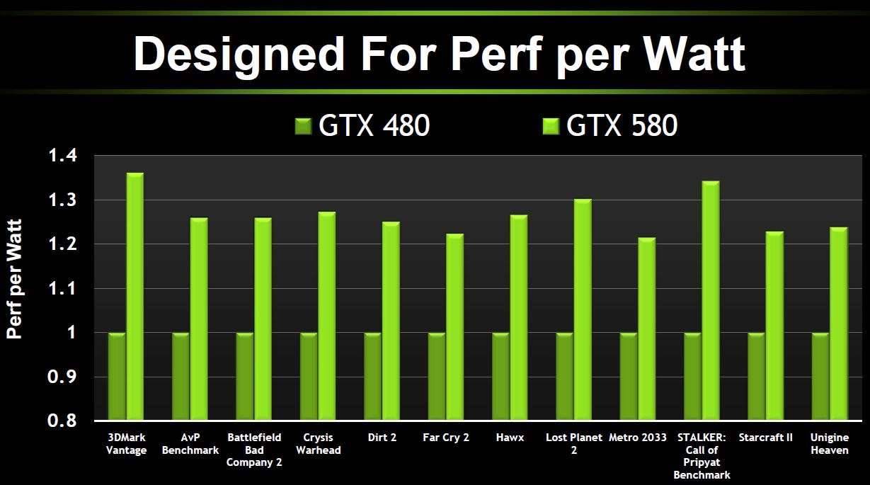
Another focus of the GTX580 is power efficiency, as Jason noted. "We’ve gone into every block of the GPU to look at all the critical timing paths, and the less sensitive timing paths, and have optimised those to reduce power – and have been able to get pretty substantial power per watt gains." The gains that NVIDIA are claiming are indeed substantial - the GTX580 is up to 30% more power efficient, an impressive feat considering the speed boost.

So we know that on paper the GTX580 is fast; but how fast is it actually?


.jpeg&h=142&w=230&c=1&s=1)


.jpg&w=100&c=1&s=0)

.jpg&w=100&c=1&s=0)
.jpg&w=100&c=1&s=0)