The pre-Christmas period seems to be infamous for graphics technology launches, and no Christmas in recent memory will be quite so frenetic as this - last month saw the announcement of the new AMD cards, and this month brings not only the announcement, but the actual launch of a new NVIDIA card: the GTX580.
Though we speculated that this is a knee-jerk reaction to the AMD cards, rumoured to launch on the 22nd of November in less than two weeks, NVIDIA insist otherwise. We spoke with Jason Paul, Product Manager for the GTX580 for the APAC region, who explained that “[NVIDIA] felt with GTX480 we could’ve done better with power and acoustics. Those were two areas we were looking at in our next generation of products”.

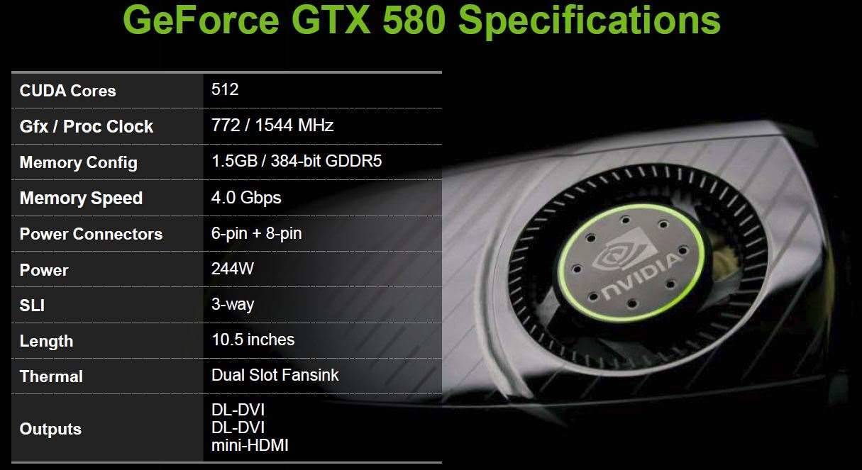
Jason continued,“GTX580 is continuing to enhance and build upon [the GTX480] with more geometry horsepower, and allows developers to create incredible terrain and characters”, and it certainly seems like they've put some hard work into the Fermi core. Official specifications have been confirmed as leaked by an overwhelming number of sites, and appear in full below:
The GTX580: back to the drawing board
As can be seen above, the GTX580 boasts the full amount of CUDA Cores possible within the Fermi architecture, suggesting that the core now sports a total of 16 functional Streaming Multiprocessors which, as we explained in our initial GTX480 review, give it a total of 512 processing cores:
Inside each GPC resides a total of four large blocks called Streaming Multiprocessors, or SMs. These SMs each contain 32 CUDA Cores, the processors that do the actual calculation work, though it appears that a single SM in the GF100 is deactivated. The fifteen functional SMs add up to a total of 480 CUDA Cores.

Though the architecture itself remains largely unchanged, the code-name is GF110; ten higher than the initial release. Its core runs 72MHz higher at 772MHz which, keeping the added CUDA Cores in mind, means this is the fastest Fermi design yet. The GTX580 also retains the same memory controller as the GTX480, which offers a 384-bit wide memory bus that connects to 1536MB of GDDR5, albeit at a significantly boosted clock speed of 4GHz vs the previous 3.6GHz.
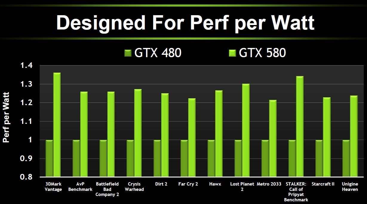
Another focus of the GTX580 is power efficiency, as Jason noted. "We’ve gone into every block of the GPU to look at all the critical timing paths, and the less sensitive timing paths, and have optimised those to reduce power – and have been able to get pretty substantial power per watt gains." The gains that NVIDIA are claiming are indeed substantial - the GTX580 is up to 30% more power efficient, an impressive feat considering the speed boost.

So we know that on paper the GTX580 is fast; but how fast is it actually?
NVIDIA GTX580 Performance Comparisons
While we'd have preferred to actually have a card to test ourselves, neither NVIDIA nor partner cards had arrived before the writing of this article. Generally we don't bother uploading these official graphs, and prefer our own more reliable testing. However there is some worthy analysis to be gleaned from the official NVIDIA performance slides included in the press presentation - but we won't be simply posting them all as given.
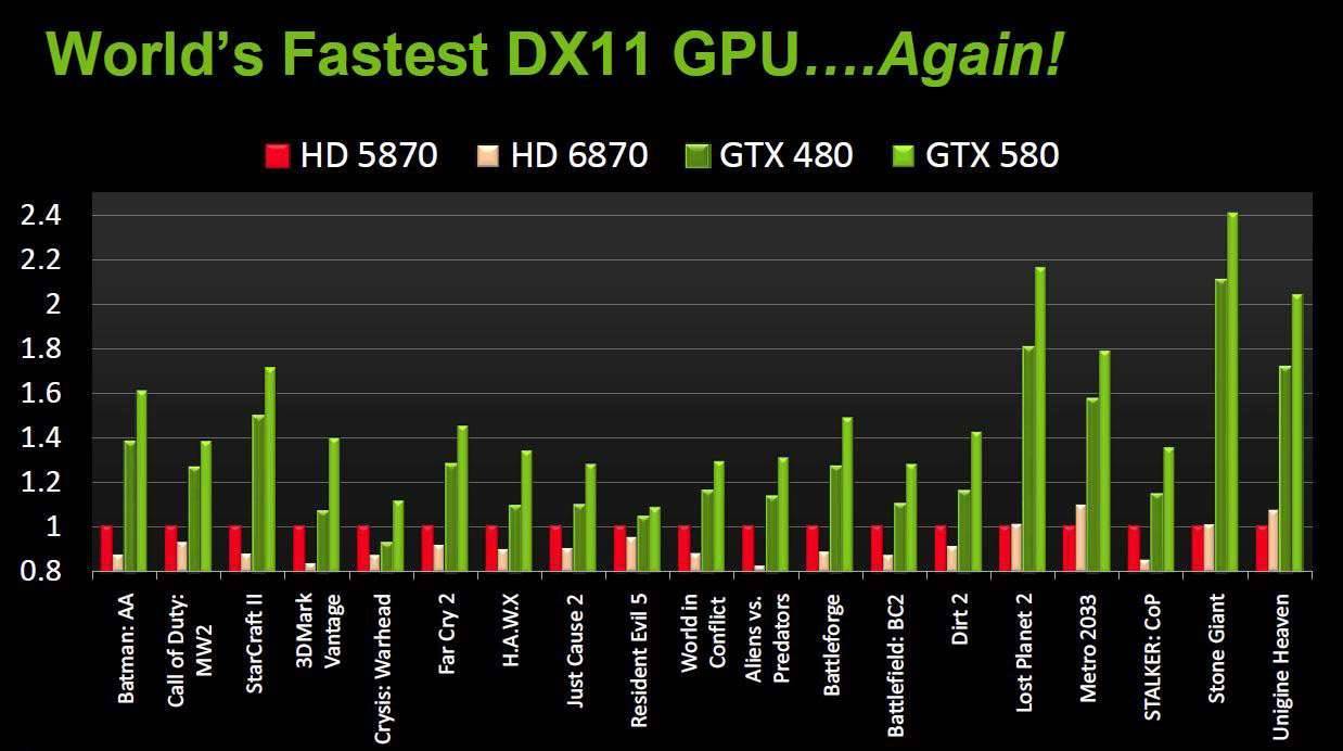
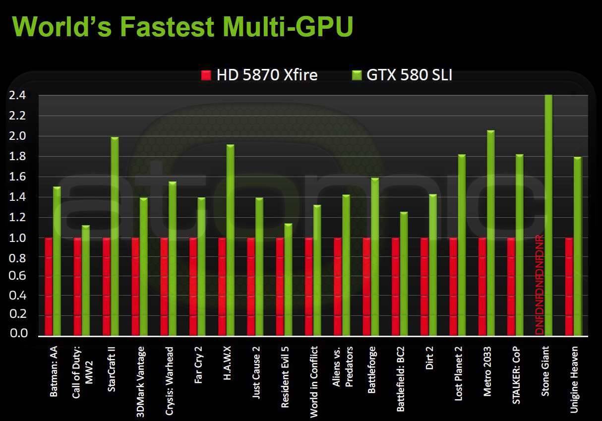
You're probably familiar with graphs such as the one below, which both AMD and NVIDIA - and indeed most of the industry - are guilty of. The graph shows a seemingly-phenomenal performance increase of one product against another, making the competing product (in this case the current high-end AMD 5870 and strangely the mid-range 6870) seem awful in comparison.
But there's one thing that is usually forgotten when looking at these graphs: the scale. As seen to the left of the graph, it doesn't begin at zero; rather beginning at 0.8. While NVIDIA was correct to standardise the results against the 5870, they didn't get the scale right - so we thought we'd fix their graphs for them. This is the untouched graph, showing an obliteration of the competition:
And here's our version of the same information:
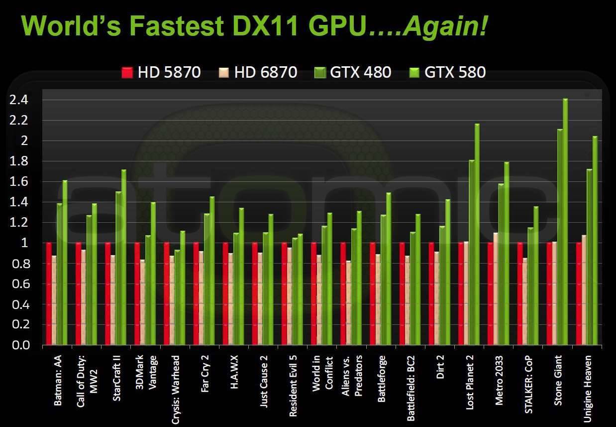
Quite a difference, isn't there? We'll let those graphs speak for themselves (our own testing has shown that the GTX480 is more-or-less equal to the 5870 in far more tests than that graph shows). But where does all this performance improvement come from, and what part of the graph should be looked at? We think the most telling comparison is to ignore the red data for now, and focus instead on the NVIDIA - the difference between those green lines isn't very much. NVIDIA helpfully pulled that information out for us in the presentation.
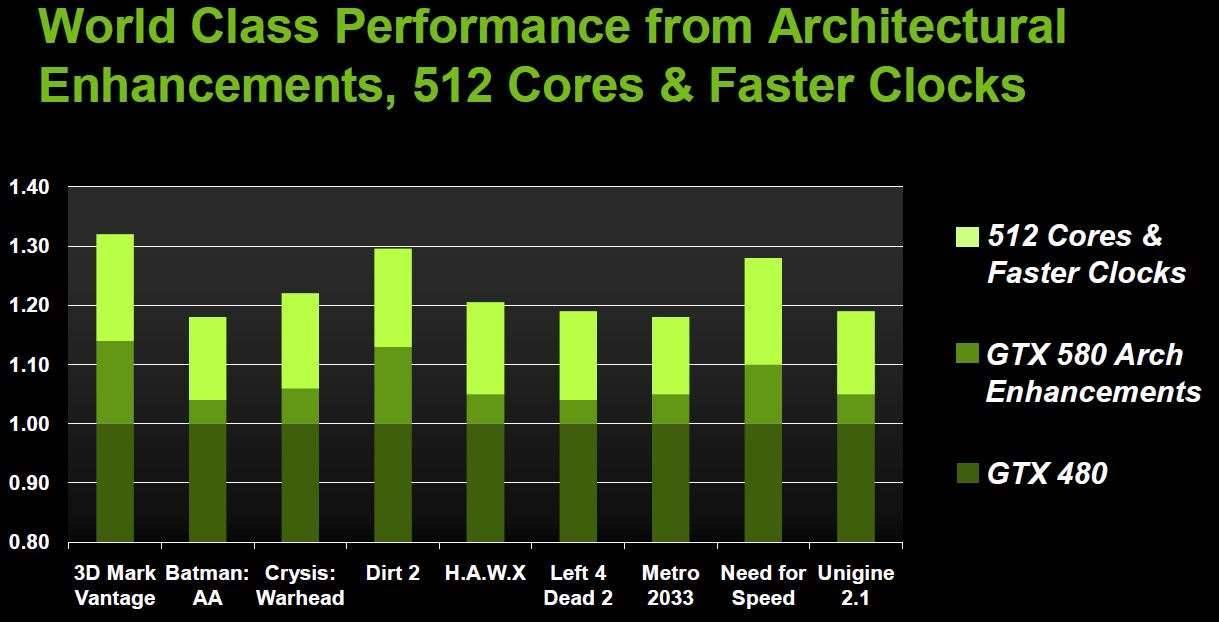
As seen in the above graph, NVIDIA reckon that at the same clocks, the GTX580 is faster than the GTX480. Called officially "Architectural Enhancements" rather than a new architecture, a boosted CUDA Core count of almost 7% accounts for most of the performance improvements seen in this graph. As for the rest, Jason explained that the GTX580 can now do “half-speed to full-speed FP16 calculation", and has "improvements in Z-cull algorithm” that give it the extra kick needed. Note that this is the same FP16 technology that NVIDIA slammed AMD over some months ago.
How does it go in DirectX 11 games?
Predictably, the NVIDIA GTX580 is a bit of a whiz kid when it comes to DirectX 11. Thanks to the hardware support for tessellation, it excels in situations when it is heavily used - which you can see to the right of this graph below. Interestingly the Civilization 5 shows a significant advantage; probably attributed to faster DirectCompute.

And finally, NVIDIA are touting great scaling under SLI, showing performance of up to two times better than AMD. It definitely looks impressive; but again, we'll have to wait until we actually have cards in our hands to confirm or reject their claims.
Read on for other improvements to the GTX580, including the heatsink and power system.
The GTX580 gets a brand-new heatsink design
The original GTX480 was infamous for its excessive thermal output. Though BIOS updates after launch mitigated some of the heat, three billion transistors chew through an awful amount of power. Thankfully NVIDIA took this into consideration when creating the GTX580 - rather than devouring a predicted 275W, it actually uses slightly less than its predecessor.
This hasn't stopped NVIDIA from thinking seriously about heat on multiple fronts, which is now going to be tackled with some new technology. Called "Vapor Chamber" if you're American, the Vapour Chamber design is one we've seen from Sapphire before - but as Jason confirmed, the NVIDIA implementation is not lisenced from Sapphire.
As seen in the below diagram, a Vapour Chamber works as part of the heatsink's base, and in the GTX580 is constructed from copper. Jason explained how it functions:
"The copper baseplate at the bottom is vacuum sealed with highly purified water, and this water goes through a cycle of evaporation and condensation, where the GPU heats up the water and it evaporates, and carries with it the heat out to the fin stacks. It condenses, and returns back to the GPU."
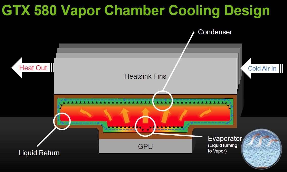
The Vapour Chamber replaces the more traditional heatpipes, though it performs the same function. This, plus the re-working of the core, has resulted in the quietest card NVIDIA have released since the GTX280!
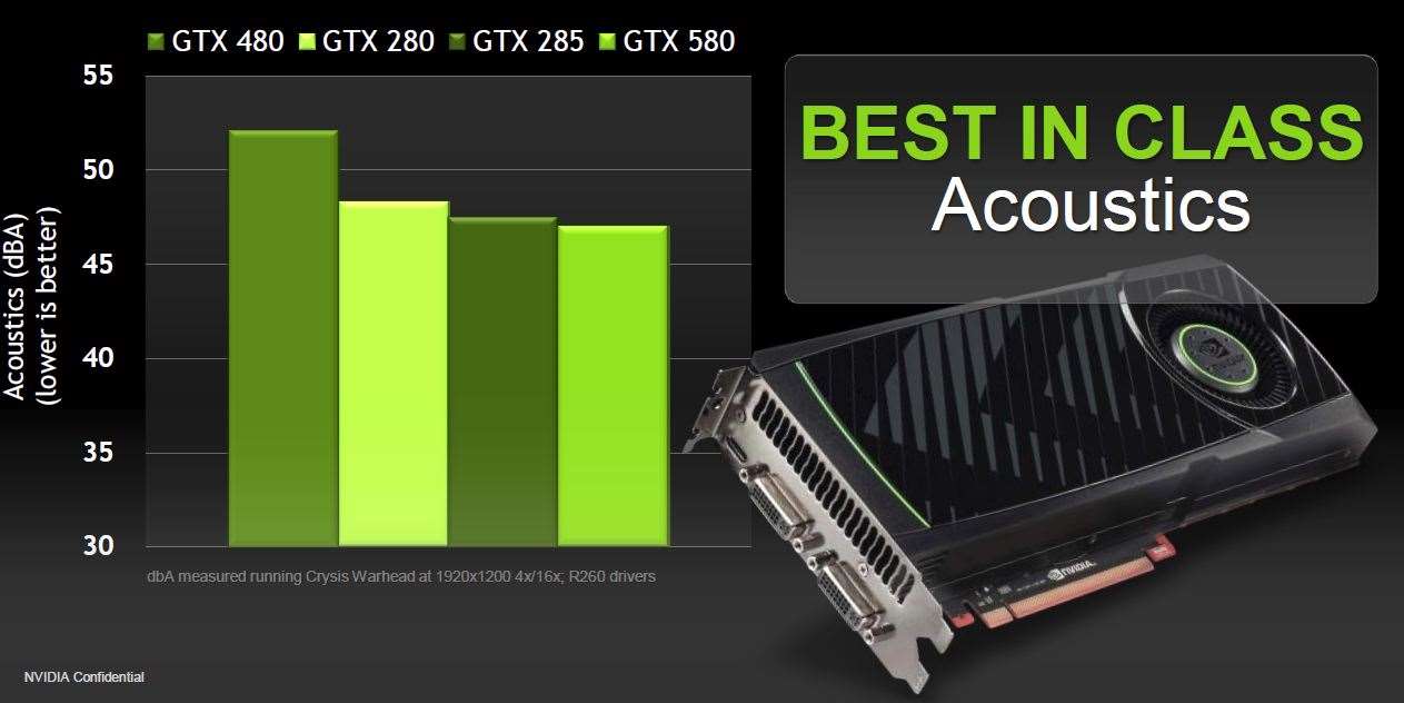
Jason was clearly proud of the new NVIDIA design, and extricated that it was quieter than "pretty much any card you look at that’s over 200 watts in the market today." That's quite a big call, but we're impressed.
NVIDIA implement power throttling under extreme loads
In a move that's sure to generate crowds of annoyed overclockers and small groups who simply don't know what it means, NVIDIA have worked some engineering magic with the power delivery system of the GTX580. In a similar way to thermal throttling of the GF110 core, where it automatically shuts down or reduces its speed to prevent damage, the power delivery system of the GTX580 will be dynamically throttled to keep the card within its power envelope - whether you want it to, or not.

Though Jason assured us that "[NVIDIA] is only doing this in certain stress applications like Furmark and OCCT, that consume power far above what real-world games produce” and that NVIDIA "didn’t want to limit overclockers”, it remains to be seen just how impactful this change is.
NVIDIA still good at tessellation, say NVIDIA
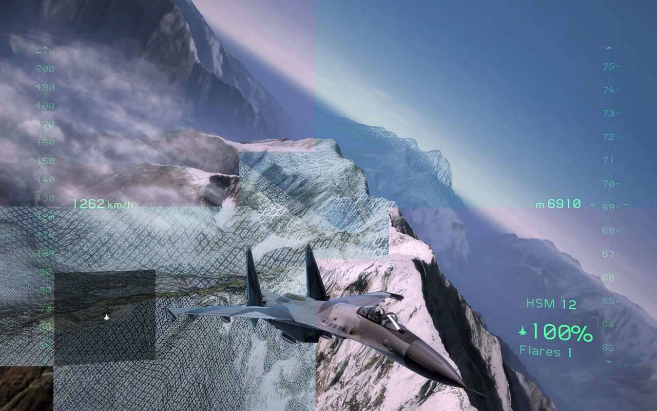
One of the last things Jason left us with was “as games take more and more advantage of [tessellation] features, our architecture really shines and comes to light in terms of the performance it can deliver. This is what we really built this GPU for; that next generation of content”. HAWX 2 highlights the kind of visual quality we can expect to see in the coming years for computer graphics:
And finally, volumes of the GTX580 card are said to be similar to the launch of the GTX480 earlier in the year, with "over 10,000 cards...already shipped into the marketplace". Jason promised that "when embargo lifts we’ll have product on shelf – this is a hard launch for us". Though we're hopeful that this is true, as of writing only a single Australian store has the GTX580 listed for a price of $682 - so if you're keen on getting one of these cards, you may have trouble.
For an idea of the variety at launch, check out our gallery of twelve NVIDIA GTX580 partner boards, which we'll update as press releases arrive.
We're looking forward to getting a GTX580 card in the Labs, and with the launch of the AMD 6970 coming soon, it's sure to be an interesting next Issue of the magazine...


.jpeg&h=142&w=230&c=1&s=1)

.jpg&h=142&w=230&c=1&s=1)


.jpg&w=100&c=1&s=0)

.jpg&w=100&c=1&s=0)
.jpg&w=100&c=1&s=0)